AMD just put a whole Zen 4 CPU inside an absolutely massive GPU
One of the most awesome developments in chipmaking in recent years has to be chiplets and stacking said chiplets on top of one another. The possibilities, as they say, are endless. AMD showed how gaming frame rates can be bolstered by stacking more cache onto a processor with the Ryzen 7000X3D CPUs (opens in new tab) at CES 2023, but it also had something equally as impressive for the data centre folks.
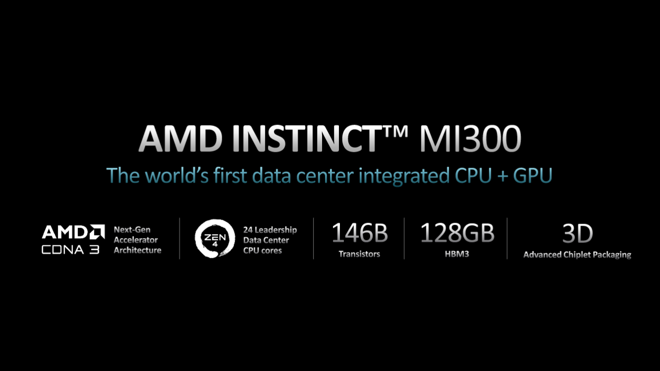
AMD is using its 3D chip-stacking tech to combine a CPU and GPU onto one absolutely mammoth chip: the AMD Instinct MI300.
It’s not just that this chip has both a CPU and GPU on it. That’s not particularly noteworthy these days—basically everything we consider a CPU nowadays has a GPU integrated into it. AMD’s no stranger either, it’s been making APUs for years—essentially chips with both CPU and GPU under one roof. That’s actually what AMD defines the MI300 as: an APU.
But what’s cool about AMD’s latest APU is the scale of the thing. It’s huge.
This is a data centre accelerator that contains 146 billion transistors. That’s very nearly double the size of Nvidia’s AD102 GPU at 76.3 billion—the GPU found inside the RTX 4090. And this thing is huge. In fact, AMD’s CEO Dr. Lisa Su held the MI300’s chip up on stage at CES and either she’s shrunk or this thing is the size of a decently sized stroopwafel. The cooling for this thing must be immense.
The chip delivers a GPU born out of AMD’s CDNA 3 architecture. That’s a version of its graphics architecture built only for compute performance—RDNA for gaming, CDNA for compute. That’s packaged alongside a Zen 4 CPU and 128GB of HBM3 memory. The MI300 comes with nine 5nm chiplets on top of four 6nm chiplets. That suggests nine CPU or GPU chiplets (looks to be six GPU chiplets and three CPU chiplets) on top of what is presumed to be the four-piece base die it’s all loaded onto. Then there’s memory around the edges of that. So far, no specifics have been given as to its actual make up, but we do know it’s all connected up by a 4th Gen Infinity interconnect architecture.

The idea being that if you load everything onto one package with fewer hoops for data to jump through to get around, you end up with a highly efficient product compared to one that’s perhaps making loads of calls to memory off-chip, slowing down the whole process. Computing at this level is all about bandwidth and efficiency, so this sort of approach makes a lot of sense. It’s the same sort of principle to something like AMD’s Infinity Cache on its RDNA 2 and 3 GPUs. Having more data close at hand reduces the need to go further afield for pertinent data and helps keep frame rates high.
But there are a few reasons why we don’t have an MI300-style accelerator for gaming. For one, reasonable expectations for most gamers’ budgets would suggest we can’t afford whatever AMD’s looking to charge for an MI300. It’s going to be a lot. Similarly, no one’s quite cracked how to program a game to see multiple compute chips on a gaming GPU as a single entity without specific coding for it. We’ve been there with SLI and CrossFire, and it didn’t end well.
But yes, the MI300 is extremely large and extremely powerful. AMD is touting around an eight times improvement in AI performance versus its own Instinct MI250X accelerator. And if you’re wondering, the MI250X is also a multi-chiplet monster with 58B transistors—but that once impressive amount just seems a little small now. Basically, that wasn’t an easy chip to beat, but the MI300 does and it’s also five times more efficient by AMD’s making.
The MI300 is coming in the second half of the year, so a ways off yet. That said, it’s more of something to marvel at than actually splash out for. Unless you work at a data centre or work in AI and have access to mega bucks, that is.
Source link


