AMD’s Infinity Links is the unsung hero of RDNA 3 and chiplet gaming GPUs


Chiplet technologies have been fully embedded into the world of CPUs with Zen 4 and Raptor Lake but are yet to reach graphics cards. But that’s all set to change with AMD’s upcoming RDNA 3 GPUs. The RX 7900 XTX and RX 7900 XT (opens in new tab) will bring chiplets to bear in gaming graphics, and to do so, the red team had to revisit its entire interconnect technology.
AMD might have mastered chiplets for CPUs, but squeezing higher performance out of a chiplet-based GPU has meant shrinking more connections into an even smaller space. That’s where something called Infinity Links comes in, which is a new fanout technology AMD is introducing with RDNA 3.
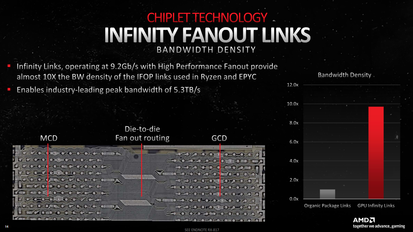
The Infinity Links fanout is used to connect the GCD die of AMD’s Navi 31 GPU package—the core graphics engine—to the MCD dies containing the GDDR6 memory interface and Infinity Cache, of which there are up to six. With this in tow, AMD is able to produce peak bandwidth of 5.3TB/s, and almost 10x the bandwidth density of the links used in Ryzen and Epyc CPUs.
“You heard the massive numbers tossed out this morning, 5.3 terabytes per second, which means we have on each one of these interfaces [MCDs] four, 64-byte channels going in both directions. That’s a lot of wires. And an organic package is not going to be able to host that number of wires,” Sam Naffziger, AMD fellow, tells me.
“We needed a new package technology and a new link technology. And that’s what we have implemented. We have named these Infinity Links and they are built on a new high performance fanout packaging technology that we have co developed with our supplier.”

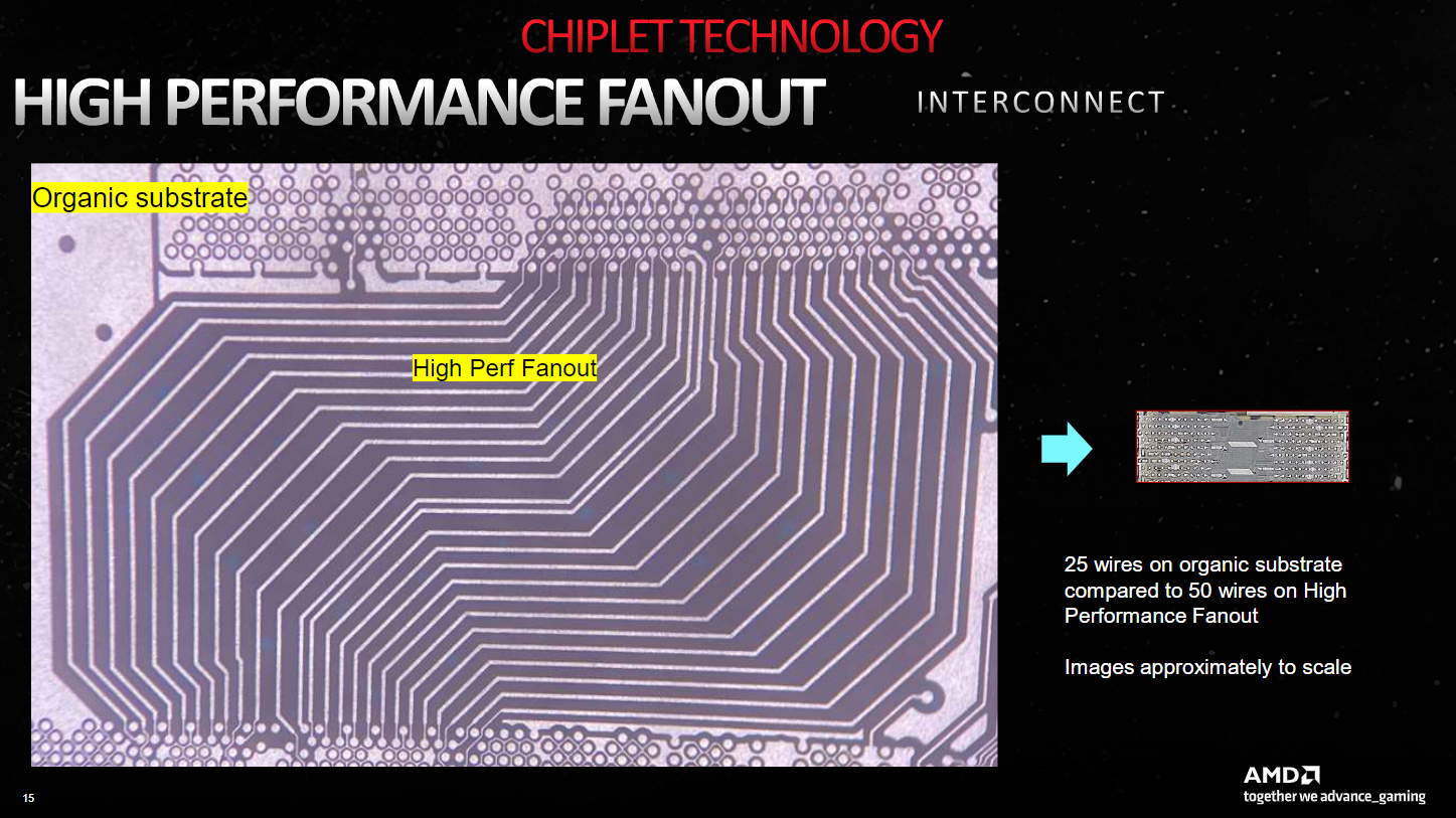
Infinity Links works by replacing the more traditional routing of traces—the layout of the microscopic wires hooking up multiple parts of a chip package—with a much, much smaller version. It’s actually quite baffling how much smaller the Infinity Link package is versus the standard solution.
Below: The traditional organic fanout is on the left, taken from one of AMD’s server products. AMD didn’t specify which, but assumedly an Epyc processor. The new Infinity Link fanout is on the right. The images are roughly to scale, according to AMD.

“The bandwidth density that we achieve is almost 10x,” Naffziger continues. “And that’s with the bit rates that you can see here, 9.2 gigabits per second signalling across these interfaces. And with the finer pitches of the bumps, and single routes, we get a dramatic increase in bandwidth density, which is exactly what the GPU needs.”
I’m told the Infinity Links interconnect alone required the effort of hundreds of engineers to get right, but that was seen as absolutely crucial work—so important as the interconnect is to the entire RDNA 3 chiplet architecture, you know, working at all.
With a view to power efficiency with the entire RDNA 3 architecture, however, the Infinity Links needed to be power efficient too. And so they are, reportedly up to 80% more efficient than organic package links due to “aggressive clock gating” and a focus on low voltage operation.
The end result: 3.5TB/s for less than 5% GPU power consumption.
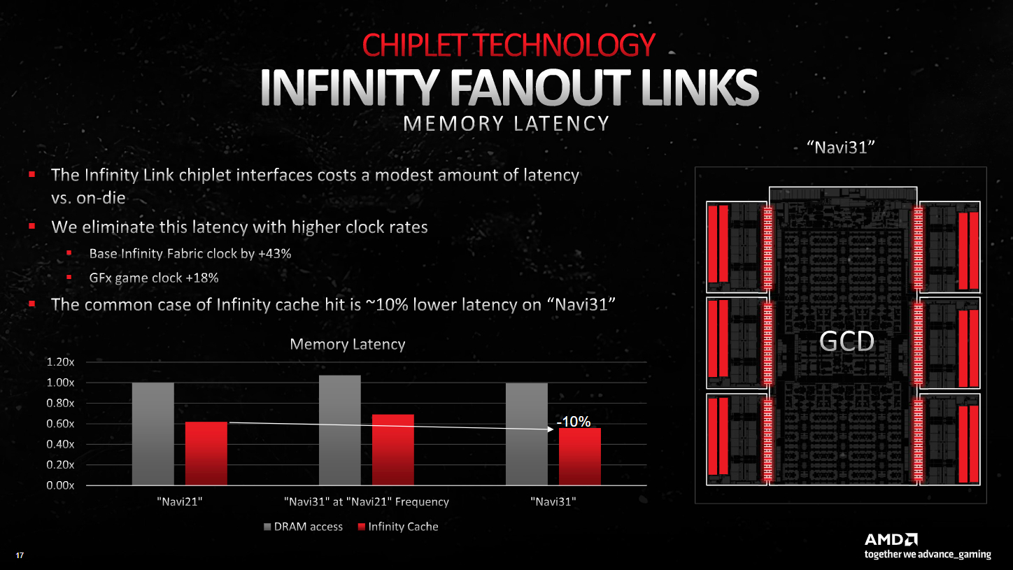
Yet in delivering a chiplet approach such as this, AMD does admit that latency has increased somewhat. Latency here means slower time to deliver a fresh frame to your monitor, which could threaten the gains from the chiplet architecture on a gaming GPU to begin with.

To combat the latency increase, AMD focused on increasing clock rates to try and negate the latency increase when sending data off the GCD die and onto one of the MCD dies.
AMD feels it’s an effective trade-off, and with a view to higher clocks and efficiency on its two upcoming RDNA 3 graphics cards, we can only hope that it’s a gamble set to pay off when it comes to frames per second. The RX 7900 XTX and RX 7900 XT will arrive on December 13, which means soon we’ll have every opportunity to see what the world’s first chiplet gaming GPUs are able to deliver for all their shiny new technologies.
Source link


