As HPC Chip Sizes Grow, So Does the Need For 1kW+ Chip Cooling
One trend in the high performance computing (HPC) space that is becoming increasingly clear is that power consumption per chip and per rack unit is not going to stop with the limits of air cooling. As supercomputers and other high performance systems have already hit – and in some cases exceeded these limits – power requirements and power densities have continued to scale up. And based on the news from TSMC’s recent annual technology symposium, we should expect to see this trend continue as TSMC lays the groundwork for even denser chip configurations.
The problem at hand is not a new one: transistor power consumption isn’t scaling down nearly as quickly as transistor sizes. And as chipmakers are not about to leave performance on the table (and fail to deliver semi-annual increases for their customers), in the HPC space power per transistor is quickly growing. As an additional wrinkle, chiplets are paving the way towards constructing chips with even more silicon than traditional reticle limits, which is good for performance and latency, but even more problematic for cooling.
Enabling this kind of silicon and power growth has been modern technologies like TSMC’a CoWoS and InFO, which allow chipmakers to build integrated multi-chiplet system-in-packages (SiPs) with as much a double the amount of silicon otherwise allowed by TSMC’s reticle limits. By 2024, advancements of TSMC’s CoWoS packaging technology will enable building even larger multi-chiplet SiP, with TSMC anticipating stitching together upwards of four reticle-sized chiplets, This will enable tremendous levels of complexity (over 300 billion transistor per SiP is a possibility that TSMC and its partners are looking at) and performance, but naturally at the cost of formidable power consumption and heat generation.
Already, flagship products like NVIDIA’s H100 accelerator module require upwards of 700W of power for peak performance. So the prospect of multiple, GH100-sized chiplets on a single product is raising eyebrows – and power budgets. TSMC envisions that several years down the road there will be multi-chiplet SiPs with a power consumption of around 1000W or even higher, Creating a cooling challenge.
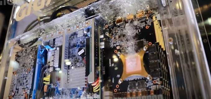
At 700W, H100 already requires liquid cooling; and the story is much the same for the chiplet based Ponte Vecchio from Intel, and AMD’s Instinct MI250X. But even traditional liquid cooling has its limits. By the time chips reach a cumulative 1 kW, TSMC envisions that datacenters will need to use immersion liquid cooling systems for such extreme AI and HPC processors. Immersion liquid cooling, in turn, will require rearchitecting datacenters themselves, which will be a major change in design and a major challenge in continuity.
The short-tem challenges aside, once datacenters are setup for immersion liquid cooling, they will be ready for even hotter chips. Liquid immersion cooling has a lot of potential for handling large cooling loads, which is one reason why Intel is investing heavily in this technology in an attempt to make it more mainstream.
In addition to immersion liquid cooling, there is another technology that can be used to cool down ultra-hot chips — on-chip water cooling. Last year TSMC revealed that it had experimented with on-chip water cooling and said that even 2.6 kW SiPs could be cooled down using this technology. But of course, on-chip water cooling is an extremely expensive technology by itself, which will drive costs of those extreme AI and HPC solutions to unprecedented levels.
None the less, while the future isn’t set in stone, seemingly it has been cast in silicon. TSMC’s chipmaking clients have customers willing to pay a top dollar for those ultra-high-performance solutions (think operators of hyperscale cloud datacenters), even with the high costs and technical complexity that entails. Which to bring things back to where we started, is why TSMC has been developing CoWoS and InFO packaging processes on the first place – because there are customers ready and eager to break the reticle limit via chiplet technology. We’re already seeing some of this today with products like Cerebras’ massive Wafer Scale Engine processor, and via large chiplets, TSMC is preparing to make smaller (but still reticle-breaking) designs more accessible to their wider customer base.
Such extreme requirements for performance, packaging, and cooling not only push producers of semiconductors, servers, and cooling systems to their limits, but also require modifications of cloud datacenters. If indeed massive SiPs for AI and HPC workloads become widespread, cloud datacenters will be completely different in the coming years.
Read MoreAnandTech


